Resistive touchscreens detect touch through physical pressure that creates electrical contact between two conductive layers. The technology operates on voltage divider principles to calculate touch coordinates.
A resistive touchscreen contains five to seven layers:
The ITO coatings have 300-600Ω sheet resistance. Spacer dots measure 0.01-0.05mm in diameter and prevent unwanted contact between layers.
Analogy: Imagine a touchscreen as a grid on a map. First, the system finds the column (x-coordinate) where the touch happened, then the row (y-coordinate). Together, the system knows the precise square on the map that was touched.
The touchscreen controller operates at a supply voltage of 3.3 to 5 volts and 3.8 milliamps.
It alternates between X-axis and Y-axis measurements at 100 to 200 cycles per second. Each measurement cycle, which includes both coordinates, requires approximately 5 to 10 milliseconds to complete.
The controller determines position using a simple voltage ratio method.
For the X-axis, the position is calculated as:
X position = (Measured Voltage ÷ Applied Voltage) x Screen Width
For the Y-axis, the position is calculated as:
Y position = (Measured Voltage ÷ Applied Voltage) x Screen Height
Analogue-to-digital converters (ADCs) digitise the measured voltages at ten to twelve bits. The touch coordinates are transmitted to the host system through standard communication interfaces (I²C or SPI).
A 10-bit ADC produces 1,024 discrete steps, while a 12-bit ADC produces 4,096 steps. For example, on a 7-inch display with a resolution of 800 x 480 pixels, a 10-bit ADC can distinguish positions to within roughly 0.8 pixels, while a 12-bit ADC increases the resolution to about 0.2 pixels.
Sub-pixel resolution doesn’t increase the visual screen detail but improves input quality. A higher resolution smoothens touch tracking, reduces jitter, and increases stylus precision. It also makes the screen compatible with higher-resolution displays, delivering more natural handwriting and motion.
In a 4-wire design, bus bars placed on opposite edges of each conductive layer create voltage gradients. The top flexible layer measures the Y-axis, while the bottom rigid layer measures the X-axis.
Both layers are actively involved in sensing, and the top layer is flexing on touch, which gradually degrades its ITO (indium tin oxide) coating. As a result, the lifespan of 4-wire panels is roughly 1-5 million touches at a single point.
In a 5-wire design, all four electrodes required to generate the X and Y voltage gradients are placed on the stable bottom layer. The top layer serves only as a passive probe and is connected by a single wire.
Although the top layer flexes under touch and wears down with use, it is not part of the measurement circuit, and the degradation of the top layer has a lower effect on accuracy.
This design makes 5-wire resistive touchscreens more durable than 4-wire versions, and they last up to 35 million touches at a single point before failure.
In an 8-wire design, the corners of the panel have two independent connections, one for driving the voltage gradient and another for sensing it. This redundancy allows the controller to take duplicate measurements for both the X and Y coordinates.
The 8-wire system can automatically correct small errors in voltage drops along long conductive traces or slight material inconsistencies by comparing the paired readings.
The compensation helps maintain accuracy, typically within ±2 millimetres, even on larger displays over 15 inches.
The added complexity makes 8-wire designs more expensive than 4-wire or 5-wire panels, but they are used in applications where consistent precision on larger touch surfaces is required.
Sensing requires an activation force between 10 and 100 grams. When pressed, the top layer deflects by 0.05 to 0.2 millimetres. The contact resistance at the touch point typically ranges from 100 to 1000 ohms.
The technology can detect touches as small as 1 millimetre in diameter. The accuracy is approximately ±3 millimetres for finger input and ±1 millimetre for stylus input.
The response time is less than 15 milliseconds from the moment of touch to the output of coordinates.
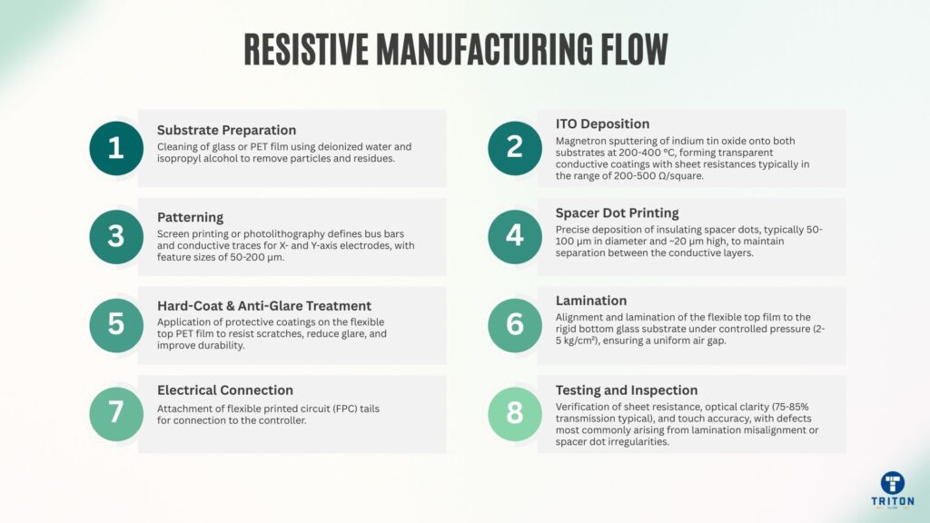
Indium tin oxide (ITO) deposition uses magnetron sputtering with substrate temperatures between 200 °C and 400 °C. The thickness of the ITO film determines the sheet resistance.
An ITO thickness of about 20 nanometers gives c. 300 ohms per square, while a thickness of about 50 nanometers reduces the resistance to around 100 ohms per square.
Post-deposition annealing is done at approximately 250 °C to 350 °C to improve the conductivity and optical transparency of the ITO layer.
The final assembly is done in a Class 10,000 or better cleanroom environment.
Automated equipment dispenses spacer dots with a placement accuracy of about ±0.5 millimetres to maintain separation between the conductive layers.
During lamination, a pressure of approximately 2 to 5 kilograms per square centimetre bonds the layers together while preserving a uniform air gap across the panel.
A key manufacturing challenge is achieving high yield. The critical process parameters are the uniformity of the ITO coating, precise layer alignment, and consistent air-gap thickness.
Deviations cause drift, dead zones, or reduced optical clarity, making process control and cleanroom discipline essential to producing reliable resistive touch panels.
Standard 4-wire and 5-wire resistive touchscreens can only detect a single touch point at a time. For multi-touch, it registers a single averaged coordinate between the contact points. Although specialised multi-touch resistive technologies exist, they require different electrode configurations and are not part of conventional 4-wire or 5-wire implementations.
Light transmission ranges between 75% and 85%, reduced by the multiple layers in the stack and the air gap. Each material interface reflects about 4% of incident light, while the air gap increases internal reflections and creates distortion at oblique viewing angles greater than 45 degrees.
Mechanical wear degrades the flexible top layer. Continuous flexing creates micro-cracks in the ITO coating, which reduces accuracy with time. Sharp or pointed objects can puncture the PET film, permanently damaging the touch function.
Operating life spans from one to five million touches for 4-wire & 8-wire panels and c. 35 million for 5-wire configurations.
Temperature fluctuations directly affect accuracy through thermal expansion. A 50 °C change causes a position drift of 0.5 to 1 millimetre. Controllers use temperature compensation algorithms to maintain accuracy across an operating range of -40 °C to +85 °C.
Projected capacitive (PCAP) technology detects touch by measuring changes in a controlled electrostatic field above the glass surface. When a conductive object like a finger approaches or makes contact, it disturbs the local capacitance at that point. The controller measures the change in capacitance to pinpoint the touch location. PCAP touchscreens are multi-touch, durable and have optical clarity of 90-92% light transmission.
PCAP became the dominant technology in consumer electronics around 2010, replacing resistive touchscreens in smartphones, tablets, and many other devices. Today, it powers all mainstream mobile devices.
Projected capacitive (PCAP) touchscreens use a grid of transparent electrodes, typically made from indium tin oxide (ITO), metal mesh, or silver nanowires.
These electrodes are arranged as a matrix of thousands of tiny capacitors. The controller applies a 100 to 250 kilohertz oscillating signal, which creates an electrostatic field that extends through the cover glass.
A finger or a stylus disturbs this field when it comes close to or touches the surface. The finger draws charge from the field, altering the local capacitance at nearby grid intersections.
The controller scans the grid 60 to 200 times per second, identifies the nodes that show a change in capacitance, and calculates the touch location with sub-millimetre precision.
There are two sensing methods:
In this method, each intersection between a row and a column acts as a tiny capacitor with a stable charge & electric field between the two electrodes. When a finger touches the screen, it interferes with this electric field and draws away some of the charge, which reduces the measured capacitance.
The controller determines the touch location by detecting exactly where the reduction occurs.
The mutual capacitance technique can accurately track 10 or more simultaneous touches, and is the standard method used in modern smartphones and tablets for multi-touch gestures such as pinch-to-zoom and rotation.
In this technique, the electrode’s capacitance is measured with respect to the device’s chassis.
When no finger is present, the electrode maintains a stable baseline charge. When a finger touches the screen, it adds conductive mass near the electrode, allowing it to store more charge and increasing its capacitance.
Self-capacitance touchscreens are about three times more sensitive than mutual capacitance touchscreens and highly responsive to light touches. However, when multiple touches occur, the system cannot always separate them. Instead, it may report false “ghost points”.
PCAP screens use several types of electrode patterns.
Diamond patterns have a 4 to 7 millimetre pitch, are uniformly sensitive across the surface and are widely used in smartphones and tablets.
Manhattan patterns use a single layer of ITO with fine metal bridges, usually 50 to 200 micrometres wide, which reduces manufacturing steps but has lower optical clarity of 90 to 92%.
Metal mesh designs use a conductive grid of very fine metal lines, typically 2 to 10 micrometres wide, instead of ITO. The sheet resistances are 5 to 30 ohms per square, compared with 100 to 300 ohms per square for ITO films. With lower resistance, the signal can travel across large panels without distortion, making metal mesh practical for touchscreens larger than 65 inches, where ITO’s higher resistance and brittleness cause performance and reliability problems.
Silver nanowire (AgNW) electrodes use a network of nanoscale silver wires coated onto a transparent film. They combine high transparency of >90% light transmission with very low sheet resistance of 10 to 30 ohms per square, comparable to metal mesh. Unlike ITO, AgNW films are flexible and cracking resistant, making them attractive for curved, foldable, and large-format touchscreens. They also don’t show the visible line artefacts of metal mesh, giving them an optical advantage in mid-size displays such as laptops, monitors, and automotive touch panels.
The sensor stack can be implemented in three main ways:
Touch controllers are typically based on 32-bit ARM processors running digital signal processing (DSP) algorithms. They digitise signals with 12- to 16-bit resolution and calculate touch positions in ~ 5 milliseconds or less, providing a highly responsive user experience.
Advanced controllers also incorporate:
PCAP touchscreens detect touch in 5 to 10 milliseconds, faster than the 16.7 milliseconds per frame of a 60 Hz display.
The responsiveness translates into tracking speeds above 3 metres per second, sufficient to capture rapid gestures, handwriting, and gaming inputs smoothly.
APCAP accuracy is ±0.5 millimetres. Modern controllers can report coordinates with resolutions up to 32,767 x 32,767, which is far higher than the pixel density of any display.
Knowledge Box: Significance of the number 32,767
A signed 16-bit integer can represent values from -32,768 to +32,767. Only the positive range is used → 0 to 32,767 for touch coordinates. That means the controller can report a grid of 32,768 x 32,768 possible coordinate points. It allows sub-pixel precision, so the system can smooth or filter touch motion and keep the controller design standard across devices of different sizes and resolutions.
The oversampling allows smooth, precise tracking even on high-resolution panels. The signal-to-noise ratio is 40:1 or better, which gives stable performance in noisy electrical environments.
Light transmission exceeds 90% because the electrode grid uses transparent conductors such as ITO, metal mesh, or silver nanowires. By comparison, resistive touchscreens achieve only 75-85% transmission.
The higher clarity of PCAP produces brighter, sharper images and better outdoor visibility.
Because sensing occurs behind the cover glass, the electrodes are never in direct contact and do not wear out even after 100s of millions of touches. Chemically strengthened cover glass, such as Corning Gorilla Glass or Asahi Dragontrail, is scratch-resistant with surface hardness in the 6H to 7H range on the Mohs scale.
Water interferes with capacitive sensing because droplets are conductive, causing false touches and preventing genuine touches from registering. To overcome this, modern PCAP controllers analyse the distinctive signature of droplets, which are large and have irregular contact areas with capacitance values that fall between those of air and human skin.
Using pattern recognition techniques and machine learning, the controller distinguishes water from a finger. Some systems can switch to self-capacitance mode in wet conditions, which turns off multi-touch but ensures reliable single-touch input even in rain.
PCAP technology uses conductive input, which means ordinary leather or wool gloves don’t work. To overcome this,
Scaling PCAP technology to larger sizes is challenging. A 65-inch PCAP sensor costs roughly 10 to 20 times more than a 10-inch version because indium tin oxide (ITO) electrodes become fragile and increasingly resistive over large areas. Manufacturers use complex electrode patterns or replace ITO with metal mesh or silver nanowires to compensate. Because of these cost and reliability issues, many large interactive displays use infrared (IR) or optical imaging touch systems instead, which are economical for large touchscreens.
Capacitive sensing is also vulnerable to electromagnetic interference (EMI) from devices like electric motors, fluorescent lighting, power supplies and wireless chargers, which generate electromagnetic fields that couple with the touchscreen’s electrodes, leading to noise and errors. Modern controllers employ differential sensing to mitigate EMI that cancels out common-mode noise, integrate shielding layers into the sensor stack, and use adaptive frequency hopping to shift away from noisy frequency bands.
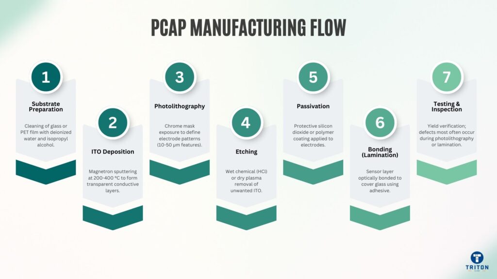
Projected capacitive (PCAP) touchscreens are manufactured in Class 1,000 or better controlled cleanroom environments to minimise particulate contamination.
The process begins with substrate preparation. Glass or PET film is cleaned with deionised water and isopropyl alcohol to remove dust and residues. Next, ITO deposition is carried out by magnetron sputtering at temperatures between 200 °C and 400 °C. Standard sputtered ITO layers used in PCAP sensors typically achieve 100-300 Ω/square sheet resistance at 50-150 nanometers thicknesses, while thinner coatings can measure up to 600 Ω/square.
Next, the electrodes are defined through photolithography, using chrome masks to create fine features in the 10-50 micrometre range, followed by etching to remove unwanted ITO, either with wet chemical processes (e.g. hydrochloric acid) or dry plasma etching.
To protect the patterned electrodes from corrosion and wear, they are coated with a passivation layer of silicon dioxide or a polymer. Finally, the patterned sensor layer is bonded to the cover glass using optical adhesive lamination, ensuring transparency and alignment.
Typical yield rates are 85-95% for rigid glass substrates, but they drop to 75-85% for flexible PET films due to alignment errors, particle contamination, and difficulties in uniform lamination. The most common defect-inducing stages are the photolithography and lamination stages.
Because of ITO’s brittleness and relatively high resistance on large areas, alternative materials like silver nanowires with sheet resistances of 20-50 Ω/square and around 85-90% optical transmission are being developed. Metal mesh electrodes are 10-30 Ω/square and scale effectively to screen sizes beyond 100 inches.
Graphene shows promise, with laboratory demonstrations achieving about 100 Ω/square at 97% light transmission, but mass production is several years away due to challenges in uniform large-area deposition.
Projected capacitive (PCAP) technology became mainstream with Apple’s first iPhone in 2007. The first iPhone introduced fluid multi-touch gestures such as pinch-to-zoom, swipe, and rotation, which were impossible on resistive touchscreens.
Consumers quickly came to expect this interactivity.
By 2012, PCAP had achieved near-total dominance in consumer electronics, with roughly 95% of smartphones and about 90% of tablets using PCAP.
The technology has since expanded well beyond mobile devices. In the automotive sector, PCAP has replaced many physical buttons and knobs with large, reconfigurable touch interfaces. Tesla’s 17-inch centre console, first introduced in the Model S (2012), is an example of this shift.
Today, all major automakers use PCAP panels for infotainment systems, climate controls, and navigation.
Banking and financial services are transitioning to PCAP technology, and even industrial equipment, dominated by resistive touchscreens due to glove use and harsh conditions, is adopting PCAP where operating environments permit. Advances like the glove mode, water rejection, and ruggedised cover glass allow PCAP to deliver the same intuitive, multi-touch experience in consumer electronics while meeting industrial reliability standards.
Together, these developments show how PCAP evolved from a consumer screen into the universal standard for touch interaction across industries.

An infrared touchscreen is built with a bezel around the display that contains rows of infrared light-emitting diodes (LEDs) on two adjacent edges and matching photodetectors on the opposite edges.
Each LED is aligned with a detector, creating hundreds of horizontal and vertical beam pairs crisscrossing just above the screen surface.
For example, a 22-inch IR touchscreen typically includes more than 1,000 emitter-detector pairs, forming a dense grid that covers the active area.
When a finger, stylus, or any opaque object touches the screen, it blocks one or more of these beams. The controller identifies the interrupted horizontal and vertical beams and pinpoints the X and Y coordinates of the touch.
Because the detection happens on beam interruption rather than a change in electrical or electromagnetic properties, infrared touchscreens can detect input from any opaque object.
Infrared touchscreens create an invisible grid of light beams across the display surface. 850 nm and 940 nm wavelengths IR are most common. These wavelengths are invisible, but special silicon photodiodes are sensitive to these wavelengths.
Infrared LEDs are mounted along two adjacent edges of the bezel, commonly the top and left, while photodetectors are mounted on the opposite edges. Each IR LED is paired with a detector, forming hundreds of crisscrossing horizontal and vertical beams just above the glass surface.
The system operates by scanning the grid. Individual LEDs are pulsed sequentially at carrier frequencies between 30 and 60 kHz, while the detectors monitor the received signals.
When a finger, stylus, or opaque object touches the screen, it blocks some beams. The controller identifies which horizontal and vertical beams are interrupted and calculates the X and Y coordinates at the point of intersection.
Modern infrared touch systems have response times of 8-20 milliseconds and a touch accuracy of about 2-3 millimetres. The higher the number of beams per centimetre, the higher the accuracy.
Advanced designs support 30 to 40 simultaneous touch points using software to distinguish multiple real-time beam interruptions.
Unlike resistive or capacitive technologies, infrared touchscreens do not require conductive coatings or transparent films. All sensing components are located in the bezel frame, and the display is covered only by standard protective glass. The design has near-perfect optical clarity, essentially 100% light transmission from the underlying display.
An infrared touchscreen system is built around four main elements integrated into a bezel frame surrounding the display.
The infrared LEDs are manufactured from gallium arsenide or gallium aluminium arsenide semiconductors. They operate at drive currents of about 10 to 20 milliamps and emit beams with a coverage angle of 20 to 30 degrees at wavelengths of 850 nm or 940 nm.
Silicon photodiodes are used as detectors because they are sensitive to infrared light. However, an optical filter is attached to their surface to increase accuracy. The filter blocks visible wavelengths and helps the screen work in bright environments.
The controller manages the LED pulsing sequence and monitors detector outputs. Modern controllers use digital signal processing (DSP) to analyse which beams are interrupted and calculate touch coordinates. IR touchscreens determine position by identifying the intersection of blocked horizontal and vertical beams. To maintain accuracy, background infrared interference from sunlight or lamps is suppressed using differential measurement and frame-to-frame cancellation techniques.
The protective screen surface requires no special conductive or sensing layers. Manufacturers use tempered glass or acrylic since infrared wavelengths pass through these materials without issue.
The bezel that houses the LEDs and detectors adds 5 to 15 millimetres to the display perimeter.
Infrared touchscreens scale efficiently to sizes above 150 inches by increasing the number of emitter-detector pairs, with grid pitch typically ranging from 3 to 10 millimetres.
At a standard 6 mm spacing, the effective touch resolution is about 50 to 100 DPI, sufficient for both finger and stylus input. Objects as small as 2 to 3 millimetres in diameter can be detected, enabling precise interaction for drawing or handwriting.
Controllers process input at scan rates that deliver 8 to 20 millisecond response times with 2 to 3 millimetres positional accuracy.
Systems designed for collaborative displays can resolve up to 32 or more simultaneous touches, using signal-processing algorithms to distinguish overlapping shadow patterns.
Unlike resistive panels, which typically respond in under 15 ms, and projected capacitive panels, which respond in 5 to 10 ms, infrared systems perform competitively despite their larger scale.
Durability is a strength of IR touchscreens. Because there are no conductive coatings or flexible films, the surface can withstand more than 50 million activations without performance degradation.
IT touchscreens have modest power requirements. Medium-sized infrared touchscreens draw less than 1.5 watts for the LED-photodiode array and controller electronics.
Operational reliability is stable across temperatures of -20 °C to +60 °C. Direct sunlight, rich in infrared wavelengths, can saturate detectors, while dust or debris on the bezel blocks beams and creates localised dead zones or phantom activations until the frame is cleaned.
Touchscreens are no longer limited to consumer devices. They are used in sectors ranging from industrial automation to automotive systems and large-format collaboration displays. The most widely deployed technologies are resistive, projected capacitive (PCAP), and infrared.
However, they are not the only available options; there are several other niche technologies.
Surface Acoustic Wave (SAW) touchscreens have optical clarity and are used in kiosks and information terminals. Optical Imaging technology like FTIR and ShadowSense are cost-effective for large screens. Dispersive Signal Technology (DST) and Acoustic Pulse Recognition (APR) detect touches through vibration analysis, making them suitable for rugged glass surfaces.
Electromagnetic Resonance (EMR) digitisers remain the standard in professional pen-input applications requiring precision and pressure sensitivity.
Each of these approaches has trade-offs in cost, durability, and performance, but together they form a complete toolkit for matching touchscreen technology to the demands of different industries.
For businesses evaluating solutions or sourcing hardware such as touchscreen PCs and industrial-grade panels, the Triton Store provides products and expertise to guide the right choice.


Melbourne
Brisbane
Phone 1300 558 438
Live Chat – Widget below
Melbourne
Brisbane
Phone 1300 558 438
Live Chat – Widget below